I’m almost in the process of preparing another article to post but my attention was diverted again to the previous 555 timer circuits I made. I simply couldn’t afford to leave the circuit that way. I am concerned that by changing the 2N3904 with the same type of transistor but of different hfe, the duty cycle changes accordingly and this is annoying.To get the correct bias voltage to pin 5 to bring the output pin 3 to 50% duty cycle without any pot or hfe requirement for the transistor is an interesting challenge for me to tackle with. Of course the simplest approach is to put an input coupling capacitor to pin 5 but doing so will eliminate the possibility of employing negative feedback to improve the frequency response and reduce distortion. But it seems the need for a pot for proper bias is somewhat unavoidable to eliminate the DC offset from the output.
My broken CRT oscilloscope is in the brink of extinction due to burned 1.5KV electrolytic filter capacitor, so my initial attempt is to rely again to LT spice simulation and compare the result in real world breadboard.
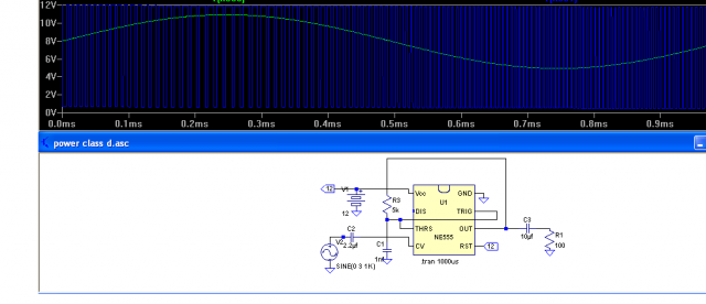
The schematic is shown below.
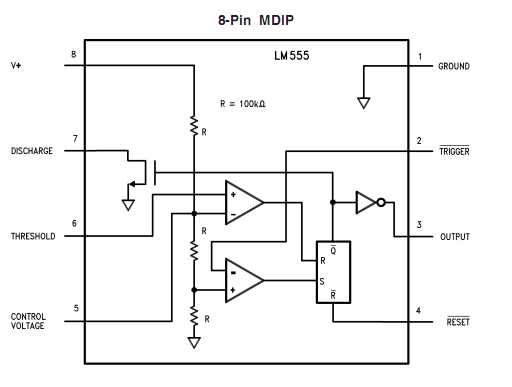
For any given supply voltage to pin 8, the voltage that will appear from pin 5 is always 2/3 of that Vcc. Since pins 6 and 2 are tied together, its oscillating voltage varies at 2/3 max and 1/3 min. At 12 V supply, pins 6 and 2 is at its threshold of 8 volts cut-off and 4 Volts cut-in respectively. If I get the average voltage of this two then I may get the desired 50% duty cycle. This statement is actually correct “if” pin 5 is open or floating. The timer will oscillate in astable mode at desired frequency but the problem usually occurs when that pin is terminated with a sound source. The impedance of the source effectively pulls down pin 5 to ground resulting to a change in frequency and duty cycle. In my breadboard the frequency drop to half, yeah I can live with that but the pain is so hard to ignore regarding the distorted sound with some noise. The circuit is shown below without transistor.
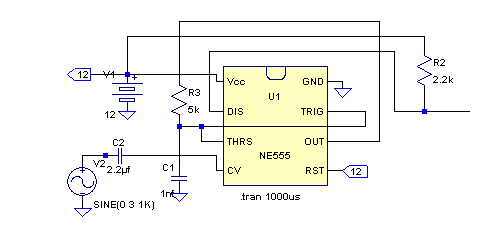
When I transferred the headphone to pin 7 with pull-up resistor, the noise disappear. This means that the source of the noise is the amplified signal from pin 3 being feedback to pin 6. So, this is the suggested output termination if someone wants to amplify the signal.
The circuit shown above has a slight reduction in volume of sound due to the high output resistance of R2 but good enough for amplification due to the absence of noise compared to first circuit.
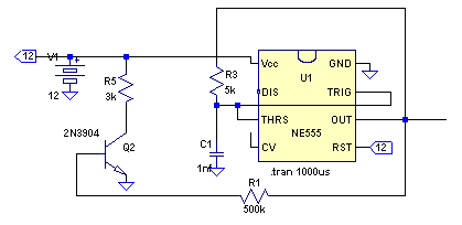
The necessity for a better sound quality and to improve frequency response is more desirable and can be achieve only by adding negative feedback (NFB). And that’s what 2N3904 comes in.
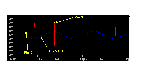
If pin 5 is not connected the 8 volts on that pin is constant while 2/3 and 1/3 Vcc at pin 6 and 2 behave in a normal astable form with 50% duty cycle.
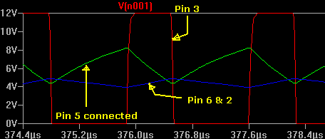
When I connect pin 5 to 2N3904 collector, the waveforms changed to both quasi triangular form with voltages at pin 6 and 2 at lower amplitude while pin 5 is higher.
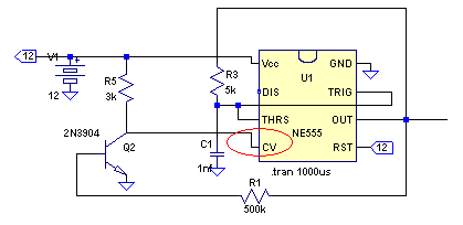 And the corresponding waveform is shown bellow
It’s quite noticeable that the duty cycle is being affected (red trace). The previous 8 and 4 Volts from pin 6 and 2 was diverted to pin 5 now with both “peaks” of green and blue voltages are functions of T rise and T fall output voltage of pin 3.
Note that by “pulling up” the green voltage i.e. the collector of 2N3904 in this case, that green will return back to its original 8 volts and the corresponding duty cycle at output pin 3 will return back to 50%. The only possible way to do this is to put a pot at the base of 2N3904, oh well here we go again, don’t laugh! I think for the time being, this will suffice until I figure out how to avoid it.
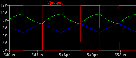
Output waveform when the pot is adjusted to a lower resistance. This means the collector current is reduced to “pull-up” pin 5 to its original 8 volts.
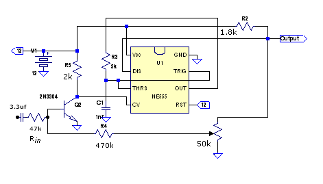
Complete schematic with pot included.
The voltage gain of the circuit above is approximately R4 divided by Rin. With an input of +/-200 mv will modulate pin 5 to +/- 2 volts. Please take note that the voltage on pin 5 should not be driven to more than +/- 2.5 volts. Doing so will produce distortion. Also, you cannot expect 100% modulation here. Based on my simulated circuit, typical modulation is something like 15 to 85% max (centered at 50%). Of course, this is only a class D toy for the beginners and should not expect full swing modulation out of it. Take note that there’s a lot of room for further improvement in this circuit such as the use of opamp that will simplify the biasing schemes.

