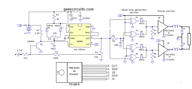
Ok, I’ve been so busy for the past few weeks and I couldn’t make a follow-up from the last article of the 555 timer circuit. So here is another improvised model circuit that will eliminate the unwanted DC offset voltage from the output that affect the previous one discussed. By the way, all previous circuits that I discussed were intended as “low power” class d amp source that is adequate to drive head phones via a coupling capacitor. This means DC offset is ignored due to the added capacitor. The schematic shown below is a reference design with added DC offset adjust pot and a high power fet driver from MICREL but I used it as a power fet substitute to simplify the amplification and cost. With this approach, there’s no need for costly fet driver with level shifter because the PWM source requires same rail supply as with the output fet. Although chip maker MICREL mentioned that MIC4451 have built-in cross-conduction minimizer, I still provide an option to include it with the use of CD4030 exclusive or gate for added safety. This will also act as phase splitter as required by the two power switchers wired in full bridge topology. I also assumed that the “would be” builder of this circuit understand several subjects like, ringings, RFI, EMI, etc. so adequate power supply by-pass capacitors and short traces of copper tracks must be implemented. Well, building a class d amp from scratch contain lots of challenge and requires courage but for some adventurous hobbyist who are bored with linear, this is worth a try.
Improvised circuit
 Edited version (October 16, 2010)
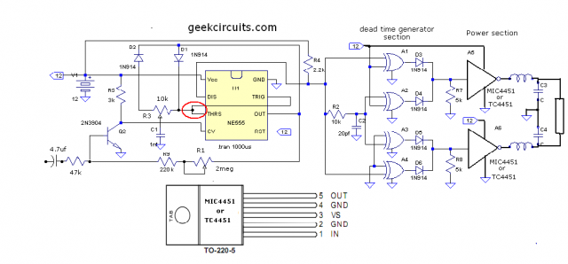
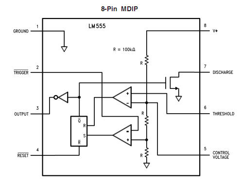
The schematic shown above requires minor tweaking on the 555 timer side due to the changes in supply voltage which is at 12 volts now. Here, aside from added offset adjust pot (50% adjust pot via R3), attention must be focused to pin 5 as well because this is the inverting input of the internal comparator which is tied-up from the voltage divider that requires tweaking also. Adjusting R1 pot will also help to accomplish this. Please refer on the schematic shown below.
555 schematic
The sawtooth voltage variations from pin 6 does not conforms to the required 2/3 VCC of the timer but instead, something less than 2/3 of VCC to obtain low distortion. For best result, adding one opamp as a replacement to 2N3904 will give better result.
Edit:
I include LTspice simulation for you to play with. Either R2 or C2 can be adjusted for dead time adjustment to the lowest distortion as possible without cross conduction. You may disregard this RC delaying network and its ORed diode resistor combination from the output and use it only as phase splitter if you like.
LT spice simulation
[smartcounter:3]


iam from indonesia.veryy good
You have 555 THRS+TRIG connected to D1+R2
shouldn’t they be connected to C1+R2 instead?
(I note that the simulation is wired as I describe)
Yes, There is a mistake in the drawing. THRS + TRIG must be connected to the center of the pot and not to D1 + R3. Thanks for correcting my mistake. I just corrected the drawing only now.
Thanks for dropping by
Dear Mr.Geek,
can u upload ur photographic view soon?